![]()
Introduction
It’s been so long since I had the idea for this project that I can’t remember why I had the idea in the first place. At least I blame it on the passage of time although this engineer is getting on a bit now so it could easily be memory rot on my part. So here we are then, a reflow oven controller. Let’s quickly recap what a reflow oven is for those that are new around here.
The two main processes used in industry to build printed circuit boards are wave soldering and reflow using a very large industrial oven that you probably can’t afford and if you could afford to buy it you probably couldn’t afford to house or run it.
![]()
Reflow on the large scale is achieved by applying solder paste to the printed circuit board using a laser-cut stencil with cutouts placed precisely where the pads are located. The solder paste itself is a mixture of flux and tiny balls of solder. A pick-and-place machine lifts the components from their packaging, e.g. a tape and reel dispenser and places them on to the board with their pads resting in the little gobs of solder paste.
The board then gets placed into the oven where a carefully controlled temperature profile is applied over the course of about 5 minutes. During this time the solder paste melts and the components ‘sit down’ into place before the solder sets as the board cools.
We can apply this basic technique to the hobbyist world with a simple plan of action. The pick-and-place machine will be replaced by my right arm and a pair of tweezers. A cost of zero so far, great stuff. Stencils and solder paste are both available to the hobbyist but the cost of the stencils are relatively high if you’re going to be making only a few boards and the solder paste needs refrigerated storage and only has a short shelf life. I’ll replace this part with a simple tinning of my boards using a soldering iron. It’ll take longer but should work just as well.
Finally we have the oven itself. Small ovens in various forms are available on ebay, amazon and they might even sell them in real shops made out of real bricks and staffed by real people. The fun part of the question is how do we make our oven follow a pre-programmed temperature profile instead of just powering up to a target temperature and staying there until the dinger goes ding and your chicken is roasted.
Of course we’re going to use a microcontroller to do it and that’s what the bulk of this article is about. Please read on.
Prior art
I’m not the first to build an MCU-based reflow oven controller and I’m probably not going to be the last. A quick google around throws up the following results, and these are just the guys that have put virtual pen to paper and taken the time to publish their work.
- Here’s an Arduino shield-based controller that looks professionally produced and generally well thought out.
- Dan Strother’s effort is a simple affair but his firmware is very good. While you’re there take a look at his Spartan-6 BGA test board. I can’t believe he did it with Eagle, there’s only so much pain a man can take.
- Sparkfun did one once and then pulled it. Goodness knows why.
- There’s even an instructable that you can follow.
There’s more. There’s a lot more, so why another one? The commercially available controllers didn’t look particularly inspiring to me so a self-build was going to be the way to go. I could either follow someone else’s schematic or come up with my own. Well I felt up to the challenge of doing it myself and bringing my own bit of flair to the presentation as well as making it highly cost-effective.
Component selection
A significant number of components need to come together harmoniously for this project to work. In this section I’ll go over the main component parts and how I selected them.
The Solid State Relay
A solid state relay (SSR) is designed to allow you to switch mains voltages on and off using low voltage DC control, i.e. a microcontroller. They do this by using an optocoupler to internally isolate the two sides from each other. When you trigger the photodiode the mains current is allowed to flow. However, it’s not quite as simple as that. The relay will only change the state of the AC output at the two points in the AC sine wave where it crosses zero so that the input and output waveforms are maintained, the zero-crossing. That imposes limits on the frequency we can use to switch it on and off, something which I will tackle in the firmware design.
![]()
The best quality SSRs are made in the USA and you do get what you pay for. There are cheap Chinese Fotek SSRs on ebay for a fraction of the cost of the USA-made SSRs. I knew I was going to need a heatsink so I got one on ebay that came with one of the Fotek’s attached. They were so cheap that I thought I’d get one just to see what they were like.
![]()
I tested the Fotek using a light load — literally — it was a desk lamp and it did what it was supposed to do, no problems there. Reports on the internet from users of the Fotek range from ‘it caught fire’ to ‘I’ve been using it for years with no problem’. I suspect that some users don’t realise that you must cool an SSR. It probably doesn’t help that the Fotek only comes with a little aluminium plate on the base that does not shout out its role as a heatsink.
I unscrewed the base to take a look at the innards but could only get it out a few millimetres without damaging the internal wiring. From what I could see there is a PCB housed towards the top of the unit and then a set of bare wires come down to the aluminium base plate where an unidentifiable component is soldered directly to it. This must be the heat generating component.
The overall cheapness of the Fotek did not fill me with confidence so I loitered some more on ebay and managed to pick up a brand new USA-made device for about £8.
![]()
The difference in quality is immediately obvious. This device is completely solid and resin-filled. It feels like a proper industrial component and a stamp on the side declares that it’s ’200% tested’. My only reservation is that the AC and DC terminals are only air-gapped. The Fotek, for all its faults, physically separates the two sides so arcing or shorting from the AC to the DC would be practically impossible.
![]()
Just look at that base plate. If you were ever in any doubt that this is a device designed to be attached to a heatsink then you won’t be after you see that. I unscrewed the Fotek from its heatsink, applied some thermal transfer gunk that I had left over from a computer HSF kit and screwed in the Opto-22 device. I’m now confident that there won’t be any smoke coming from my mains control unit.
The temperature sensor
After doing some research it turns out that the most popular IC for handling the amplification and analog to digital conversion of the thermcouple readout is the MAX6675 and its successor, the MAX31855 from Maxim. The two devices have the same footprint and pinout but are not software compatible and may not all work with the same thermocouples.
The MAX6675 can read a range of 0 to 1023°C with 0.25°C resolution. The MAX31855 extends the capabilities by being able to read below zero but it adds the limitation that the thermocouple must not be grounded. The MAX6675 can be grounded and in fact it must be grounded if you want to take advantage of its ability to sense an open (disconnected) state. I decided to design the board to be able to handle either type of sensor IC using a jumper to ground it and I’ll be using the MAX6675 on my own build.
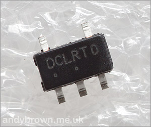
A defective MAX6675
The MAX6675 (and its successor, the MAX31855) are rather expensive little chips but I noticed that they were available on ebay for just a few pounds so I bought one. Mistake. I wasted about half a day trying to figure out why the readings I was getting from it were scaled up by a factor of 8. It just didn’t make any sense.
I couldn’t just say, yeah whatever and write my software to scale down by 8 because the maximum reading would be 128°C which is way too low for a reflow oven. This issue had to be resolved.
Eventually I decided to try removing it from the board and replacing it with one that I got from a different seller on ebay that had slightly different numbering printed on the case, perhaps indicating a different batch. It worked perfectly. Lesson learned, it’s just not safe to buy ICs on ebay because you don’t know where they’re sourced from. Next time I’ll swallow the cost and stick to the usual major name suppliers that I usually use.
Anyway, in case it helps anyone else here’s a picture of the bad IC. If you’ve got one with the same ‘+120′ numbering and it’s misbehaving then drop-kick it into the waste bin and replace it with one from a reputable supplier.
![]()
Now that the sensor is selected I’m going to need a compatible thermocouple…
The thermocouple
Thermocouples have different designations depending on the temperature range that they are designed to handle. If you’re interested, Wikipedia has a complete list of all the types. The MAX6675 sensor requires a ‘K’ type thermocouple which has a range of -200°C to +1350°C, far more than we will ever need. ‘K’ type thermocouples are available on ebay for just a few pounds and the user feedback for them is very good so I bought-one-now and waited forever for it to arrive from China.
![]()
This is a grounded thermocouple. That is, there is electrical continuity between the blue wire spade terminal and the cable braid and the outer metal end of of the sensor itself. This will work with the MAX6675 but I’m not at all sure that you’ll be able to use it if you choose the MAX31855.
The controller
All of the components listed above need to be linked together with an MCU-based controller board. The basic requirements of the controller board are as follows:
- Accept user control input.
- Provide user feedback via a display.
- Interface with the MAX6675 temperature controller.
- Implement a PID algorithm to control the state of the SSR.
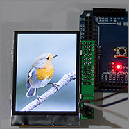
I decided to integrate a Cortex M0 MCU with the 640×360 TFT LCD from the Sony U5 Vivaz mobile phone. If you haven’t already done so then you can read all about my prior efforts in reverse engineering that display in this article. The graphical user interface will be supported by an 8Mbit SPI flash device from Spansion.
![]()
The 3.2″ Sony Vivaz LCD
When I started this design there were a couple of aspects where I was operating on a hunch that things would work out. Firstly, the STM32F051C8T7 MCU comes with 64Kb flash. I wasn’t sure whether that was going to be enough to hold the debug builds of the firmware that I would need to do in-circuit debugging with my ST-Link/V2 debugger.
Secondly, I wasn’t certain that the SPI flash interface was going to be fast enough to create a responsive user interface. I really dislike sluggish user interfaces, only instant responses are acceptable to me. The killer feature here is the DMA channels linked to the SPI interface in the STM32F0. If I run the SPI interface at 24MHz (the fastest available) then I should be able to get a 1.5 megapixel/sec sustained transfer rate using DMA because each pixel is 16-bits wide. That should be enough for a responsive UI but I will only know for sure after it’s too late to go back.
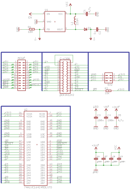
Controller schematic
![]()
Click on the thumbnail to see the full schematic PDF. I’ll go through the each section of the schematic in detail but first lets take a look at the bill of materials.
| Designator |
Description |
Footprint |
Quantity |
Value |
| BOOT0, RESET |
Push-to-make button |
PCB button |
2 |
|
| C2 |
Capacitor |
0603 |
1 |
56pF 50V |
| C3 |
Capacitor |
0603 |
1 |
56pF |
| C4, C8 |
Capacitor |
0603 |
2 |
2.2µF |
| C5, C15, C17 |
Capacitor |
0603 |
3 |
1µF |
| C6, C7, C11, C12, C13 |
Capacitor |
0603 |
5 |
100nF |
| C9 |
Electrolytic capacitor |
Radial 2x6x6 |
1 |
10µF |
| C10 |
Tantalum capacitor |
1206 |
1 |
22µF |
| C14 |
Capacitor |
0603 |
1 |
10nF |
| C16 |
Capacitor |
0603 |
1 |
10nF |
| C18 |
Capacitor |
0805 |
1 |
1µF 50V |
| C19 |
Electrolytic capacitor |
Radial 2x6x6 |
1 |
100µF |
| C20 |
Electrolytic capacitor |
Radial 2x6x6 |
1 |
4.7µF |
| C21, C22 |
Capacitor |
0603 |
2 |
100nF |
| D1, D2, D4 |
ESD Suppressors |
SOD-923 |
3 |
OnSemi ESD9B5.0ST5G |
| D3 |
Schottky Rectifier |
SOD123 |
1 |
B0530W |
| DEBUG |
Header, 10-Pin, Dual row |
2.54mm pitch |
1 |
|
| FB1, FB2 |
Inductor |
0603 |
2 |
BLM18PG221SN1D |
| L1 |
Inductor |
CDRH5D28 |
1 |
22µH |
| LCD |
Panasonic connector |
AXE534124 |
1 |
(only digikey US) |
| Left, Right, OK |
PCB terminal block |
2 pin |
3 |
|
| MCU |
Header, 3-Pin |
2.54mm pitch |
1 |
|
| ON: SENSE, USART |
Header, 2-Pin |
2.54mm pitch |
2 |
|
| POWER |
PCB terminal block |
2 pin |
1 |
|
| PWR SEL |
Header, 2-Pin |
2.54mm pitch |
1 |
|
| Q1 |
TSM3442 MOSFET |
SOT26A-6AN |
1 |
|
| Q1.1 |
Generic MOSFET |
SOT23-3N |
1 |
|
| R1, R2, R3, R7, R8, R9, R10, R11 |
Resistor |
0805 |
8 |
10kΩ |
| R4, R5, R6 |
Resistor |
0805 |
3 |
1kΩ |
| R12 |
Resistor |
0805 |
1 |
100Ω |
| R13 |
Resistor |
0805 |
1 |
5.1Ω |
| SPI |
Header, 5-Pin |
2.54mm pitch |
1 |
|
| SSR |
PCB terminal block |
2 pin |
1 |
|
| U1 |
2.8V LDO regulator |
SOT353-5N |
1 |
ZXCL280H5TA |
| U2 |
3.3V regulator |
SOT223-4N |
1 |
AMS1117 |
| U3 |
8Mbit serial flash |
SOIC8N_N |
1 |
S25FL208K |
| U4 |
ARM Cortex M0 |
LQFP48_N |
1 |
STM32F051C8T7 |
| U5 |
Thermocoupleto A/D Converter |
SOIC127P600-8AN |
1 |
MAX6675 |
| U6 |
Backlight boost converter |
SOT26A-6AN |
1 |
AP5724 |
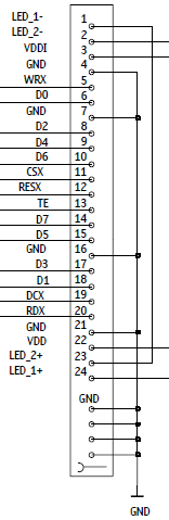
The LCD interface
![]()
This is a direct copy of the connector schematic from my Vivaz reverse engineering article. It’s a proven design so the decision to drop it into this schematic is an easy one to make. The Vivaz backlight is a string of six white LEDs in series. We have to provide the power for that string but the R61523 controller in the Vivaz LCD has a programmable PWM output that we can use to provide a programmable brightness by connecting that PWM output to the enable pin of the voltage boost converter.
![]()
TFTs always need two voltage inputs, one for the digital interface and one for the analog display driver. If you’re lucky they’re both the same and fit the same range as your MCU. We’re not so lucky with the R61523. The digital interface will take 3.3V but the analog voltage requires 2.8V. That’s no problem, we just drop in this small and cheap regulator.
![]()
That string of 6 white LEDs in series needs 19 point something volts to light up. The best way to do that is with a constant current backlight generator such as this AP5724 from Diodes Inc. The feedback resistor R13 sets the desired current to 20mA and the EN pin allows us to vary that down to provide a dimmer function.
The power regulator
![]()
3.3V power is provided by an AMS1117 3.3V regulator. The maximum current output, 1A, is way above what we will need but the main reason for selecting this regulator is its high input range of up to 15V. I’ve bought some illuminated panel buttons for the physical case that require a 12V input to light up so I’ll be able to use a single 12V input to power the controller board and illuminate the panel buttons.
The ESD diode is optional and can be omitted if you trust your 12V input power supply. The AMS1117 will operate quite happily with just the 22µF output capacitor but I took a belt-and-braces approach and added a 10µF electrolytic capacitor to the input side as well. In this design the power supply needs to be smooth because of the sensitivity of the MAX6675 to noise so the output capacitor should be chosen carefully. I chose a tantalum device because they perform just as well as a ceramic in this role and are more cost-effective in the 22µF size.
![]()
The PWR SEL jumper allows me to isolate the AMS1117 from the controller board. Why would I want to do that? When I need to program the SPI flash with the graphics for the UI I will connect up an STM32 development board and use it to program the flash. When I do this I will need to power my board from the same supply as the STM32 development board. The 3-pin MCU header allows me to do this but I must also isolate the AMS1117 because voltage regulators don’t like to receive a reverse current on their output pin. The 3-pin header also has an MCU_RES pin that is connected to the RESET pin of the Cortex M0. When I’m programming the flash using an external MCU I will connect this pin to ground so that the Cortex M0 is held in a reset state and does not try to initialise and interfere with the programming session.
The MAX6675
![]()
This module handles the MAX6675 interface. The power, ground and SPI connections are all so-so, nothing special there. However the the T+ and T- inputs to the device are handled with some care. I’ve made provision for filtering the inputs using a 10nF capacitor and ferrite beads as well as protecting the device with ESD protection diodes. All of these features are optional and may be omitted from the final design but it doesn’t hurt to get the footprints for the filtering components on to the board just in case we need them.
The SENSE jumper block allows the T- terminal to be grounded when the jumper is connected. When the MAX6675 is grounded it is able to sense if the thermocouple becomes disconnected. I use this feature in the firmware to provide an emergency abort if the thermocouple link is broken during the reflow process.
If you plan to use the successor to the MAX6675, the MAX31855 then this jumper must be left in the OFF position because that device does not like being grounded. Although I do have a couple of 31855′s in the workshop I have elected to use the simpler 6675 in my implementation because the 31855 comes with some limitations on the type of thermocouple that you can use.
The SPI flash
![]()
The Spansion flash device is connected up using a standard SPI interface. This device supports ordinary 1-bit SPI output and also a fast dual-output mode that uses both MOSI and MISO to output 2 bits per clock. If we were using an FPGA then we could use this feature to double the output data rate. However the MCU SPI peripheral doesn’t understand this proprietary feature so we will be using 1-bit mode at 24 megabits/sec.
The debugger
![]()
This 20-pin header is designed to interface directly with the JTAG cable that comes with the ST-Link/V2 debugger. The ST-Link/V2 will be used to upload programs as well as mediate between an OpenOCD server and the Cortex M0 MCU using ST’s SWD protocol so that I’ll be able to do full IDE debugging using Eclipse.
BOOT0 and RESET buttons
![]()
Having a reset button is a convenience just in case I need to force an MCU reset. The pin is pulled up since reset is active low and a small capacitor provides some protection against transient dropouts causing a spurious reset.
I decided to include a button that would allow me to control BOOT0 just in case I wasn’t able to get SWD debugging to work. If BOOT0 is high when the MCU is reset then it will boot from the internal bootloader which can then download a flash image from the USART pins. I hoped I wouldn’t need this but it does give me another way to flash the device if SWD didn’t work (it did work…)
The input buttons
![]()
This design will feature three buttons for navigating the user interface. There’ll be a left, right and an OK button. I considered, and rejected the idea of a touch screen because when I operate this device my hands will be dirty and a touch screen would quickly become fouled up. The three buttons will be ‘active high’ so they are pulled down and get connected to 3.3V when the user presses the button.
The MCU
![]()
Here’s the heart of the system, the STM32F051C8T7 MCU in an LQFP-48 package. These MCUs are extremely competitively priced. For £2.60 + tax at Farnell you get a 48MHz 32-bit ARM MCU with 64Kb flash, 8Kb SRAM, loads of on-board peripherals and a DMA controller. You don’t even need an external oscillator as long as you can accept up to 1% deviation from the stated clock speed. They’re even available for less than a pound at Future Electronics and if it wasn’t for their punishing international delivery charges that’s where I’d get them from.
We’ll use all of port B for the LCD 16-bit data bus. That means with the help of an optimised assembly language stm32plus driver I’ll be able to push pixels to this device at 12MHz because the Cortex M requires 2 clocks to write to a GPIO pin and we need to do that twice per pixel write-cycle. 12MHz, or 83ns is very close to the maximum supported by the R61523 LCD driver which is very handy for us.
PA0..2 are mapped to the LCD control signals. PA5..7 correspond to the SPI1 MCU peripheral pins and PA3 and PA4 are the chip select signals for the SPI flash and the MAX6675, respectively. We will share the SPI1 bus between the flash and the 6675 and use the chip-select signals to choose which one we are talking to at any one time.
PA9 and 10 are mapped to the MCU USART1 peripheral TX and RX. I mentioned earlier on that I would use the USART to flash the MCU via its bootloader if I had problems with the SWD debugger. In the end I did not have any SWD problems so I decided to use the USART as a way of exporting reflow session data as a CSV file to a connected computer.
PC14, PF0 and PF1 handle the button inputs and PA11 is the output control pin for the SSR.
The VDD and VSS (ground) connections as well as the decoupling capacitors all follow ST’s recommendations.
The SSR output
![]()
The relay output is a simple on-off switch which I’m implementing as a logic level N-channel MOSFET. A high level pulse on the gate will cause 3.3V to flow through the SSR’s control pins and back to ground. We already know that the SSR has a 1kΩ resistor between its control pins so we don’t need to add any more resistance of our own.
I happen to have quite a few TSM3442 MOSFETs in stock so that’s the one I’m using. However, it does come in a rather obscure SOT23-6 footprint when nearly all the competitors come in a SOT23-3 format. To make it easier for others to implement this design I’m including footprints for both devices on the PCB and you just need to use the footprint that fits the device you can obtain.
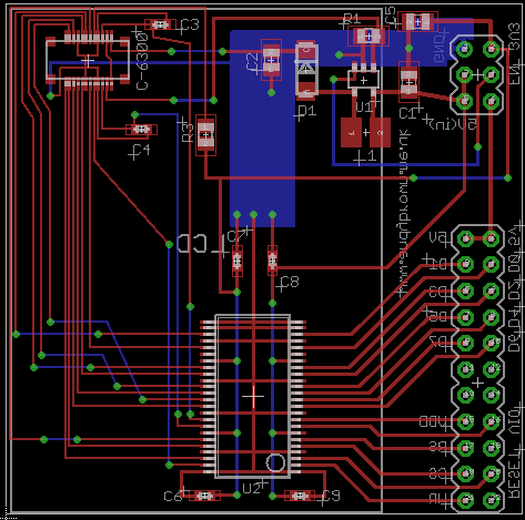
The PCB design
With the schematic compiled and ready it’s time to start laying down the PCB footprints and traces. The LCD panel measure 80x45mm and I want the PCB to double as a mounting base for the LCD so I’m going to work on a 100x100mm PCB board size. Here it is.
![]()
PCB design thumbnail, click for PDF
On one side there is the LCD and its connector. The physical layout of the LCD panel is such that when the LCD is facing upwards the connector is facing downwards which makes it easy to mount on to the board. This is the side of the board that is designed to be pressed up against a window cut out from the box in which the board will be mounted. The other side of the board contains all the components and connectors. This will face down into the box and therefore be accessible for debugging purposes.
The highest frequency signals are going to be between the MCU and the flash and the MCU and the LCD therefore these signals are kept as short as possible. The MAX6675 needs to be kept safe from noise so it’s placed away from the digital components and its power line takes as direct a route from the regulator as possible and there is an unbroken ground plane beneath it.
I generated gerber files from the design and uploaded them to Elecrow for printing. Other, similar services from ITead and Seeed Studio are available but I’ve had good service from Elecrow and their prices are the best (at the moment) so I continue to use and recommend them.
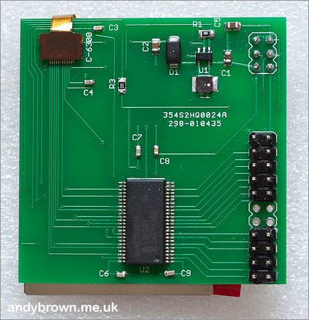
After the usual multi-week wait for the slow postal service to deliver the boards they arrived safely and every one’s a winner as far as I can see. Click on an image for a larger version.
![]()
Most of my vias are large and untented because you never know when you’re going to need an impromptu probe test point on your board but there are some tented vias around the LCD connector where there would be a danger of the FPC tail coming into contact with the circuit board.
These tented vias are necessarily small otherwise the solder mask will just fall into the hole instead of tenting over the top. Unfortunately the reality of these cheap prototype services is that total tenting is very hit and miss, usually the mask does cover the annular ring but then collapses into the hole.
![]()
Note that these boards do not feature the Q1/Q1.1 dual-footprint option for the SSR MOSFET switch that I talked about earlier. I added that to the design after these had been printed.
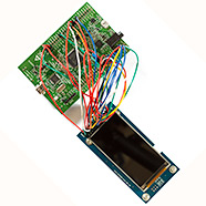
Now it’s time to build it. The build was straightforward in that there’s nothing on there that I haven’t soldered before but there are rather a lot of components and there is the additional complexity of components that require reflow on both sides of the board.
The way I dealt with that problem is to reflow the board in stages using my hotplate. The LCD connector on the reverse side went on first as it’s probably the most troublesome with its 0.4mm pin pitch. After that was down I divided the top of the board into sections containing ICs that could be reflowed one section at a time by holding the board partially on the hotplate so the part with the LCD connector fitted to the back hung off the edge.
![]()
![]()
After the ICs were reflowed into place I then went back to my hot air gun for the SMD passive components and a normal iron for the remaining through hole parts. As you can see from the image above it all worked out rather well. Let’s have a look at the board modules.
![]()
The AMS1117 is closely accompanied by its supporting electrolytic and tantalum capacitors. The PWR_SEL jumper in the foreground is normally on, allowing power to come from the external 12V wall adaptor. When programming the flash device from an external MCU this jumper should be OFF to prevent the AMS1117 from seeing a reverse current on its output pin. The 3.3V/GND/RESET header is then used to apply power from the board that’s being used as the programmer and the RESET pin is tied to GND to prevent the Cortex M0 from ever coming alive while programming is taking place. You can’t achieve this by isolating the power pins because the voltages that the MCU sees on its IO pins will cause it to unexpectedly power up — you have to hold it in the reset state.
![]()
The AP5724 backlight boost converter circuit and its associated inductor and schottky diode. The output capacitor C18 is going to be seeing around 19V so it needs to be rated accordingly. I used a 50V rated 0805 part.
![]()
The STM32F051C8T7 MCU and the 4.7µF electrolytic capacitor recommended by ST. This MCU does not require an external oscillator, the clocks are generated from an internal 8MHz oscillator trimmed by ST to around 1% accuracy. Soldering the LQFP-48 part was remarkably easy. To most people the legs on these ICs look the same but having soldered so many different ICs I can tell you for sure that some are made of metal that attracts solder much more readily than others. This IC is one of them. Just add flux, touch the legs and the solder runs up those legs like its magnetically attracted. I’ve seen the same with Xilinx FPGAs and it’s a real relief when a device behaves like that.
![]()
The 20-pin header originally specified for JTAG. For every signal there is a neighbouring ground line. Very good for minimising crosstalk on a parallel cable but very profligate on pin usage. We are going to be using ST’s Serial Wire Debugging (SWD) protocol which only requires a small number of pins that you can see labelled on the board here. The pinout is designed to match the 20-pin cable that comes with the ST-Link/V2 debugger and the little bump in the silkscreen aligns with the bump on the cable connector.
![]()
The Spansion flash device is placed close to the MCU, keeping signal lines short and helping with signal integrity. It’s placed at a 45° angle because that’s just the way it worked out so that the traces were the shortest they could be.
![]()
The MAX6675 footpring is accompanied by a jumper that determines whether the T- pin should be grounded or not. For the MAX6675 this needs to be ON so that the open circuit state can be detected. For the MAX31855 this must be OFF. In my design I left space for ferrite beads and ESD diodes but in the end I did not need them as I get a nice clean reading without them so the ferrites are replaced by 0R resistor bridges and the ESD diode footprints are left blank.
![]()
The SPI breakout header allows me to access the two SPI devices for testing and, for the flash device, programming with an external MCU. When programming the flash I hardwire nCS_OVEN to 3.3V so that it can’t interfere with the programming process.
![]()
The navigation buttons break out to terminal blocks at the edge of the PCB suitable for wiring directly to a momentary push-to-make button. A pull-down resistor causes the unpressed state to be GND and a small-ish series resistor helps to smooth out unwanted noise from the button contacts.
![]()
The output terminals for the SSR control pins break out to a standard screw terminal block. The actual (small) load is switched with a logic level MOSFET. You can see the TSM3442 in the photograph with its unusual SOT23-6 pinout. This photograph was taken before I added the choice of footprints between this one and the more standard SOT23-3.
![]()
The two switches allow me to manually reset the MCU and also to control BOOT0. The ability to reset is useful during debugging but not essential and can be omitted. Controlling BOOT0 was part of my belt-and-braces approach to being able to flash the board. I wasn’t 100% certain that my SWD interface was going to work so I needed a way to cause the MCU to use its internal bootloader to source the flash image from the USART pins as a failsafe. In the end though the SWD interface worked perfectly so this BOOT0 switch is redundant and can be omitted.
![]()
In the above paragraph I explained why I might have needed access to the USART pins for programming purposes but since that scenario did not come to pass I was left with a couple of potentially useful pins looking for a purpose. What I did in the end was program the firmware to have an option to output the (T,degrees) points from a reflow curve to the USART so that they can be viewed on a computer charting program.
The firmware
Time to write the firmware and for me that’s definitely the fun part. I decided to use my own stm32plus C++ library to take the strain out of interacting with the hardware and to allow me to just get on with producing a good interface.
I decided that the interface would feature a main setup ‘control’ screen where you can change the reflow parameters followed by an ‘action’ screen that would actually perform the reflow according to the parameters I’d defined. Time to fire up Photoshop and create a mockup UI that would serve as a template for my control screen.
![]()
Click for full 640×360 size
This full size 640×360 mockup allowed me to extract and save the individual graphics, including all the numeric characters saved as graphics against their correctly coloured backgrounds. These graphics will be converted to a raw format by the stm32plus bm2rgbi utility and then uploaded to the Spansion flash device on the controller.
The tiled format, with apologies to Microsoft, gives a nice and clear UI that I will be able to navigate around using the three buttons on the controller. The SnPb and SnAgCu tiles allow me to select between lead and lead-free profiles. The mockup shows both tiles checked because I’ll need to save out both those check-boxes to flash due to the different coloured backgrounds (the graphics are anti-aliased by photoshop against the background colours and I need to preserve that).
The purple reflow buttons takes us to the ‘action’ screen. The grey ‘flame’ button shows a constantly updating readout of the current oven temperature which is useful during the cool down phase.
The blue buttons allow me to adjust the co-efficients of the PID algorithm. The defaults will be 1/1/1 and after simulating the algorithm on my PC I know that I only need to be able to move up and down in integer steps to increase or decrease the effect of each component of the algorithm.
The selected parameters are saved to a page in the flash memory and are automatically restored on power-up.
You have to be careful when selecting a font due to commercial licensing issues that cover most of those very nice looking ones that come with Windows so the font that I used throughout is Titillium Web from the Google open source web fonts project.
Fast SPI graphics
There’s three words you don’t often see used together. Surely a 1-bit interface is never going to be fast enough for interactive graphics? Well, it is. By running the SPI interface at the fastest 24MHz rate offered by the MCU and utilising DMA to transfer big blocks at once we achieve bursts of 1.5 megapixels/sec. This is more than fast enough to update just the changing parts of the display in real-time.
My implementation is realised by a FlashGraphics class that initialises the SPI interface on construction and de-initialises it on destruction. This allows me to freely write graphics or read a temperature from the oven even within the same function without having to care much about who owns the SPI bus. The bus is owned by whichever controller class happens to be in scope at that time.
Here’s the main drawBitmap method from the FlashGraphics class.
  /*
   * Read the bitmap from SPI and write it out to the display
   * We'll use the Read Data (03H) command because our max frequency of 24MHz
   * is lower than the device's max of 44MHz so we don't have to use the Fast Read
   * command that would incur a speed penalty due to the dummy writes.
   *
   * The strategy here is to use DMA to read in the bitmap from the flash device into
   * a buffer in chunks. When half the buffer is full we transfer it to the display
   * while DMA is filling the remainder. When DMA has filled the remainder we transfer
   * it to the display. This allows us to get a good utilisation out of the SPI bus.
   *
   * Note that in master mode the SPI clock will not tick unless we transmit something.
   * Without a ticking clock the flash slave device will not latch out the data. Therefore
   * we use DMA to "transmit" fake zero bytes just to get the clock to tick so that there
   * will be data for us to receive. This is one of the oddities of ST's SPI implementation
   * that you just have to learn.
   */

  void FlashGraphics::drawBitmap(const Rectangle& rc,uint32_t offset,uint32_t length) {

     uint8_t zero,bytes[4];
     Panel::LcdPanel& gl(_panel.getGraphicsLibrary());
     Panel::LcdAccessMode& accessMode(_panel.getAccessMode());

     // set up the drawing rectangle and get ready for receiving data

     gl.moveTo(rc);
     gl.beginWriting();

     // first 32-bits are the read command and the offset

     bytes[0]='\x3';
     bytes[1]=(offset >> 16) & 0xff;
     bytes[2]=(offset >> 8) & 0xff;
     bytes[3]=offset & 0xff;

     // select our device

     SpiNssManager nss(*_spi);

     // write out as four 8-bit transfers

     _spi->send(bytes,4);

     // get a temporary buffer and set the dummy byte to zero

     uint8_t buffer[READ_BUFFER_SIZE];
     zero=0;

     while(length>=READ_BUFFER_SIZE) {

       // start a read and wait for half complete

       _rxdma.beginRead(buffer,READ_BUFFER_SIZE);
       _txdma.beginWrite(&zero,READ_BUFFER_SIZE);

       while(!_rxdma.isHalfComplete());

       // transfer the first half to the display while the other half is finishing off

       accessMode.rawTransfer(buffer,READ_BUFFER_SIZE/4);

       // wait for the full complete

       while(!_rxdma.isComplete());

       // transfer the second half

       accessMode.rawTransfer(&buffer[READ_BUFFER_SIZE/2],READ_BUFFER_SIZE/4);
       length-=READ_BUFFER_SIZE/2;
     }

     if(length>0) {

       // receive and transfer the remainder synchronously

       _spi->receive(buffer,length);
       accessMode.rawTransfer(buffer,length/2);
     }
   }
To prove the theory I set up my logic analyser to capture the DMA transfer. You can see the results in the screenshot below.
![]()
Click for larger
The serial clock is ticking at a continuous 24MHz while the data is being latched out of the device on the MISO line. This is all as expected and validates this part of the design nicely. I’ve documented the process for flashing the graphics to the IC in the readme page that accompanies my github repo.
The reflow page
When the desired reflow profile and parameters have been chosen the purple ‘reflow’ icon takes us to the page where all the action is. This is a separate and distinct area of the firmware. All memory used by the control page is freed and the reflow page is constructed to take its place.
![]()
Click for full 640×360 size
Again I mocked up how the page might look in Photoshop before starting the coding. All the necessary graphics were saved off and added to the UX resources that would be written to the SPI flash memory.
When the user lands on this page the oven is off and we’re ready to go. At this time the user can activate the ‘go’ icon which is selected by default or the ‘exit’ icon can be activated to return to the control page.
Assuming the user hits go then the action starts. The PID algorithm will be repeatedly run to select a low-frequency PWM signal for the halogen lamp as the algorithm attempts to track the reflow profile. The actual temperature will be displayed in orange just below the desired temperature. A red-line will plot across the chart to show how the oven is performing.
The PID algorithm
The Proportional, Integer, Derivative (PID) control algorithm is documented at length on the internet so I won’t go over how it works again here. The actual algorithm itself is very simple indeed. The core of my PID implementation is shown below and can also be seen here and here on Github.
  /*
   * Update the algorithm with the current error and get a percentage value back
   * that can be used as a PWM duty cycle (0..100). This method should be called at
   * a fixed time interval.
   */

  uint8_t Pid::update(variable_t desiredTemperature,variable_t currentTemperature) {

    variable_t error,pwm,derivative;

    // current error term is the difference between desired and current temperature

    error=desiredTemperature-currentTemperature;

    // update the integral (historical error)

    _integral+=error;

    // the derivative term

    derivative=error-_lastError;

    // calculate the control variable

    pwm=(_kp*error)+(_ki*_integral)+(_kd*derivative);
    pwm=Max(Min(100.0,pwm),0.0);

    // save the last error

    _lastError=error;

    // return the control variable

    return static_cast<uint8_t>(pwm);
  }
The datatype used by the algorithm can be either fixed or floating point (a variable_t typedef in my code above) and that means we have a choice to make. The lazy man’s default choice is the IEEE double type that’s built into the C++ language. It’s a shame that the built-in type manages to be the worst performing choice without hardware assistance and, being a binary fraction suffers from accuracy issues that serve to trip up the unwary.
So now that I’ve slated it I decided to be that lazy man and see whether it would do for me or whether I would need to optimise. Sure enough as soon as the double type and the necessary calculations were added the firmware size jumped up by 8 Kbytes in debug mode. A fixed-point implementation could surely knock that down to less than 1 Kbyte but wasn’t necessary because I was nowhere near the 64Kb flash size limit and it would have been a case of premature optimisation.
Logo screen
With so much of the MCU and external flash resources still available I decided to design a logo screen to show for a few seconds when the device powers up. Out came Photoshop again and after an hour or so of faffing around here’s what I came up with.
![]()
Click for larger
The logo graphic is DMA’d from flash to the LCD whilst the backlight is switched off and then I fade up the backlight, hold for a few seconds then fade back out, construct the ‘Control’ screen and fade back in again. The end result is a smooth transition between states.
Final code size
With everything enabled and using inefficient double-precision numbers for the PID algorithm, here’s the resulting code sizes.
| Mode |
Optimisation |
Text |
data |
bss |
| debug |
none |
44268 |
2128 |
1144 |
| fast |
-O3 |
41568 |
2128 |
1144 |
| small |
-Os |
25592 |
2128 |
1144 |
The debug size is the most important because if that one breaks through the MCU limit then I won’t be able to attach to the running instance and debug it with Eclipse and gdb. The small size is particularly impressive, just 25Kb is needed for an optimised version of the firmware.
PWM and the SSR
A zero-crossing SSR such as the Opto-22 device that I’m using cannot be operated with a high-frequency PWM signal in the same way that you can dim an LED. The only way to do it reliably is with an external zero-crossing feedback circuit and a pulse-density algorithm. Essentially it would work like this:
- Each second, run the PID algorithm and get a percentage density for the next second. Distribute 1′s and 0′s evenly across 1 second according to that percentage density that you have. For example a 100% density will result in 100 1′s for people in a 50Hz mains country. A 50% density would result in 100 alternate 1′s and 0′s. A 25% density would result in 0-0-0-1 repeated until you’ve got 100 digits. Reset your interrupt’s index position to zero.
- Hook up the zero-crossing detection line to an external interrupt (EXTI on the STM32). It should fire at twice your mains frequency.
- When the interrupt fires pick the 1 or 0 from the array you created at the interrupt index position. If you get a 1, switch on the SSR, a zero will switch it off. Increment the interrupt index position and reset it to zero if you hit the end of the array.
I don’t have a zero-crossing feedback signal in my design but that wasn’t going to stop me trying the above algorithm anyway with a fixed 100Hz interrupt. It didn’t work reliably at all. It seems you really do need to be in sync with the actual zero crossing.
No matter, although it would have been nice to dim the halogen lamp it’s not really necessary. The heat-up/cool-down speed is so slow that you can easily just use a PWM signal with a low frequency (I chose 2Hz). The length of the on-off periods in a 2Hz signal is high enough to span a lot of zero crossings so it doesn’t matter if you miss one at the start or the end.
The hardware build
The controller’s built, the firmware’s written. Now it’s time to put it all together and test it in the real world.
The oven
![]()
Click for larger
This is the halogen oven that I bought. It cost about £25 on ebay for a 12 litre model rated at 1300W. When it arrived it was bigger than I thought it would be. 7 litre models exist but I chose the larger 12 litre model because they come with the more powerful 1300W bulb that I thought I might need to get the temperature up as high as I need it to go.
Halogen versus toaster oven. Why choose halogen? Lots reasons put together really. Toaster ovens aren’t as common in the UK as they are in the USA, halogen ovens are very common and low cost. Halogen ovens heat up faster than toaster ovens and that’s important for the ramp-up stage of the reflow profile. Halogen ovens have amazing visibility. Not only is the whole thing glass but there’s that extremely bright halogen lamp as well. Let’s take a look at the modifications that I’ve made to the oven to make it reflow-friendly.
Mounting the thermocouple probe
The thermocouple probe needs to be mounted inside the oven and it comes with a screw connector near the probe end that can be used to secure it to the inside of a frame. The problem is that the halogen oven is entirely glass and that means I’m going to have to grind a hole in the side of it.
Grinding a hole through glass is remarkably easy. You just need a rotary tool and a diamond-coated engraving and drilling bit. I bought this set on ebay.
![]()
It comes with all manner of bits for engraving and grinding. This is the one to use for grinding a hole through glass.
![]()
The procedure for boring the hole is that you need to use your rotary tool on its lowest speed and you must keep the grinding area wet. I marked a point on the edge of the bowl just slightly above the higher of the two internal metal stands and then I put a large drop of water on that spot and set about grinding through. The water forms a white paste with the ground glass which helps to grind further down as well as protecting your bit from damage. I worked slowly and was soon through the bowl without any hassle. I then had to spend a few more minutes working the hole larger by rotating the bit around and grinding outwards until the hole was large enough to take the thermocouple.
![]()
There it is, no cracks or splinters. It really is easy to grind through glass if you take it slowly.
![]()
And there it is with the thermocouple screwed in and ready so that only the probe is exposed to the heat and not the cable that runs back to the control unit. The probe is positioned just above the stand so that it will sense the temperature within millimetres of the board surface.
The controller housing
I decided to mount the controller inside an ordinary black project box. A rough hole was cut in the front panel where the LCD would show through. The rough edges were then masked with a black square of thin plastic film with an accurate cutout for the LCD visible area. Then I placed a 10x10cm square of clear acrylic over the top and the four screws go all the way through the panel and the PCB mounting holes.
![]()
Click for larger
Further holes were drilled for the buttons, the 2.5mm SSR cable, the 2.1mm power cable, the power button on the back and the thermocouple cable. Insulation tape is wrapped around the back of the thermocouple cable to prevent the metal braid from shorting anything in the box.
![]()
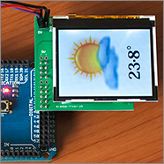
Here it is switched on. The front panel buttons are illuminated and the control page is being displayed. It’s notoriously difficult to photograph an LCD display and this photograph does little to convey just how bright and colourful it is in reality. The controller box feels very light in the hand, maybe I should glue a brick inside to give it that ‘quality’ feel ![:)]()
The AC control unit
![]()
|
You’re an engineer, you don’t need to be warned about the potentially lethal dangers of working with your household mains supply do you? Stay safe, learn why and how.
|
In my design I have elected to separate the SSR and its mains interface away from the sensitive low voltage MCU controller and particularly the MAX6675 thermocouple AD converter. That means that I need to find a second chassis that is safe to house mains current. I chose to use an old computer PSU from a long forgotten AT-format computer that was languishing on a shelf in my garage.
![]()
A computer power supply case is ideal for this task because it’s designed to handle mains voltage, has an earth post on the chassis, and it has an in-built fan for cooling. Furthermore, these old AT supplies come with a passthrough connector that was intended for your monitor. In my design this outlet will be used for the oven routed internally via the SSR. I discarded the 80mm 12V DC fan that came with the PSU and replaced it with a 240VAC 80mm fan that I found on amazon.
![]()
I noted that the power connectors are rated for 10A but the oven comes with a 13A fuse in its wall plug. It would be a bad idea for the connectors to melt before the fuse blows so I decided to fit a 10A fuse into the wall-plug.
I wasn’t immediately certain how many amps a 1300W oven would draw until I searched around on the internet and found that the camping fraternity were successfully using these ovens at sites that have 10A limits along with all their other kit without tripping the circuit breakers. Halogen lamps are filament lamps and so they should be almost purely resistive with a power factor close to 1.0. That means that the current draw at 1300W ought to be around 5 or 6 amps.
![]()
Here’s the PSU chassis after I modded it to hold the mains parts of my project. The SSR is screwed to the heatsink which is screwed to the bottom of the chassis. The yellow wires are the control signals that connect back to the control box with a 2.5mm ‘headphone jack’ cable connected into one of the existing holes in the PSU chassis that originally held one of the power cables.
The perspective of the photograph makes that 2.5mm socket look a lot closer to the mains SSR terminals than it actually is but still I would prefer to have a physical barrier over those mains terminals and indeed Opto22 do sell a cover separately. I may do something about this issue later but at least for now I know that the chassis is earthed all the way back to my house supply which is itself protected by a very sensitive RCD board.
Testing
For my first test run the oven was unmodified except for the hole where the temperature probe is fitted. The firmware performed as expected, which was a relief, and the P-I-D co-efficients were set to 1-1-1.
![]()
It should be evident from the photograph of the display at the end of the run that we have some problems that need to be solved.
- The ramp up time is too slow meaning that the oven cannot keep up with the profile. There could be a few reasons for this.
- The surface of the glass, particularly the top, gets very hot. This heat loss can be addressed with the addition of some insulation material.
- There’s a metal guard below the lamp that must be there to shield the lamp from fat spatter when the oven’s being used to cook food. The guard is drilled but nonetheless it serves to reflect back a significant portion of the lamp’s output.
- The PID algorithm doesn’t react fast enough to the cooling down phase at the end. I can address this by simply stopping the process at the end, or perhaps tuning the P-I-D coefficients. P (the present) needs to be more significant than I (the past) to make it react faster to change.
So there I was watching the above test run and in the background my wife was peering in with that ‘now what’s he up to?’ look on her face. The test finished and I was muttering to myself about heat loss and how I was going to have to go off to B&Q to see if I could find some oven insulation. “Why don’t you line it with tin foil?” came a voice from over my shoulder. You know what, that might just work was what I thought.
![]()
So I lined the bottom and sides of the bowl with foil, shiny side inwards, leaving the top uncovered so I could get a good bird’s eye view of the board being cooked and then I re-ran the test when everything had cooled back down to room temperature. Did it work? Hell yes! At 100% power the ramp up rate is much faster than that required by the reflow curve and it easily reaches the peak temperature.
![]()
After playing with the PID variables I settled on 30/1/1. These values result in a very close tracking of the target curve.
![]()
As you can see cooling is still an issue and with no way to automatically vent heat – all I can do is cut the power – the best way to achieve the cool down phase is to simply lift the lid of the oven. That’s what I did in the above test run. I also modified the firmware to make it not advance time until the 25° profile starting temperature is reached.
Fan modding
There’s a metal AC fan in the lid of the oven that operates at a constant high speed while the oven is operational. It’s designed to circulate the hot air to help cook food quickly and evenly. I want to keep the fan so that heat is distributed evenly but the problem is that it’s so strong that it blows small components clean off the PCB. I need to modify it.
I first thought about slowing it down using an inline capacitor but on closer inspection I noticed that the fan is actually two fans on the same spindle. Up above the inner fan there’s another set of blades inside the housing that I can just see through the vents in the plastic. It’s obviously there to cool the electronics from all that heat below and that’s a valuable feature that I want to keep. I decided to modify the lower fan blades to reduce their impact on the PCB in the oven.
![]()
Here’s the unmodified fan. I decided that the easiest thing to try would be to bend the blades from their default steep angle to a much shallower angle. That should result in less air being moved and the air that is moved ought to create a circular vortex around the outside of the bowl.
![]()
As you can see the modifications are not too drastic and leave me room to flatten the blades further if necessary but in my first test an 0603 capacitor placed on a dry PCB didn’t move at all during the entire test run so I don’t think I’ll need to compress the blades any more.
Watch the video
I put together a video of the oven executing the SnPb reflow profile. You can see it by clicking on the player below. Alternatively, click here to view it on the youtube website.
The video shows the oven during one of its test runs. There’s a small test PCB inside the oven with some 0603, 0402 and 0201 components placed at strategic locations to check that the fan doesn’t blow them away. The embedded close-up of the controller shows how well the oven tracks the reflow profile. The ideal track is in green, the actual track is in red. The panel at the top right shows the actual temperature, ideal temperature and the 2Hz PWM duty cycle being applied to the oven’s mains supply by the SSR.
Source code and Gerbers
The source code’s available from Github. It’ll work with the MAX6675 out of the box. If you want to use it with the MAX31855 then you’ll need to create an equivalent to Max6675TemperatureReader.h and Max6675TemperatureReader.cpp then change the typedef for DefaultTemperatureReader to reflect the name of your new class. I’ll happily accept a pull request for this modification.
The Gerber files are available from my download page. These will be accepted as a 10x10cm board order by any of the usual suspects such as Seeed, ITead or Elecrow.
Final words
This has been a fun project, the outcome of which has provided me with a real enabling tool that will make all my future builds much controlled and repeatable than they ever have been before. I mean, I was getting pretty good with a hotplate but there was no way the plate heating ever followed a standard profile and the danger of burning the bottom of the board that is in contact with the plate was always just a few seconds away.
If you’re considering building your own reflow oven and have any questions or comments on what I’ve presented here then please feel free to leave a comment or send me a message using my website contact form.


 The SSD1963 is another one from Solomon Systech. It’s slightly unusual in that it’s not hard-wired to any particular resolution. Instead it allows you to program it to support any resolution up to 800×480 as long as you know the timings for the panel that you’re going to use.


 Unlike some other devices such as the 8-bit AVRs the STM32 doesn’t have any EEPROM memory included on-chip although it is possible to emulate it to some extent by reading and writing the internal flash memory at runtime.